Semiconductor Lithography
The pattern-transfer processes used to define nanoscale electronic structures repeatedly across semiconductor wafers.
- Revision
- 1
- Created by
- SCIENDIA Knowledge Desk
- Updated by
- SCIENDIA Knowledge Desk
- Last updated
- 18.08.2026 12:20
Built by the community
Members can improve this article. Every saved change remains visible in the revision ledger.
Overview
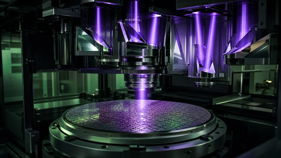
Lithography projects or writes geometric patterns into a light-sensitive resist so that subsequent deposition, etching and implantation create transistors and interconnects. Modern manufacturing repeats this cycle across many aligned layers with nanometre-scale tolerances.
Technical foundations
Optical projection follows a resolution relation involving wavelength and numerical aperture, with process factors determined by illumination, mask and resist. Extreme-ultraviolet lithography uses approximately thirteen-and-a-half-nanometre radiation and multilayer reflective optics because materials absorb strongly at that wavelength. Masks are reflective and operate in vacuum. Chemically amplified resists multiply photon-driven reactions during post-exposure bake, improving sensitivity while introducing diffusion and stochastic variation. Multiple patterning can divide dense layouts across exposures when one image cannot meet pitch requirements.
How it works
A mask and optical system form an aerial image in resist. Exposure changes solubility, development reveals a pattern and process steps transfer it into underlying films. Extreme-ultraviolet systems use reflective optics, while computational correction reshapes mask features to compensate diffraction and process effects.
Measurement and research methods
Metrology uses critical-dimension scanning electron microscopy, optical scatterometry and overlay targets to track wafer variation. Aerial-image simulation and optical proximity correction reshape masks so printed edges approach design intent. Process-window experiments vary focus and dose, while defect inspection must find rare mask, particle and resist failures across large area. Statistical process control links exposure, bake, etch and deposition measurements. Line-edge roughness and stochastic missing or bridged contacts require distributions, not just mean feature size, because one defect can disable a circuit.
Key ideas
- Printed feature size depends on wavelength, numerical aperture and process control.
- Overlay error between layers can matter as much as single-layer resolution.
- Defect probability must be controlled across billions of repeated structures.
Current research frontier
Research develops high-numerical-aperture extreme-ultraviolet systems, improved resists, computational lithography and directed self-assembly. Chiplet integration and three-dimensional stacking alter how scaling value is assessed but retain demanding pattern and overlay needs. Machine learning accelerates mask optimisation and defect classification while requiring physics and fab-specific validation. Open challenges include source power, mirror lifetime, mask inspection, photoelectron statistics and escalating capital cost. Sustainable manufacturing must also address energy, ultrapure water and process-chemical use per functional device.
Why it matters
Lithography enables continued improvements in computing, memory and sensors and integrates optics, plasma physics, chemistry, precision mechanics and statistical process control.
Limits and open questions
Short-wavelength sources, masks and resists are expensive and complex. Stochastic photon and chemical variation create rare defects, and smaller features increase sensitivity to contamination, line roughness and thermal-mechanical drift.
Explore through connected concepts
This article is indexed with 20 technical tags. Select a tag to explore the Wiki by concept.
You may also explore
Recommended from the technical tags shared with this article.
Battery Recycling
Processes that recover materials and functional components from spent batteries for safe treatment and renewed production.
Read article →