Semiconductor Lithography
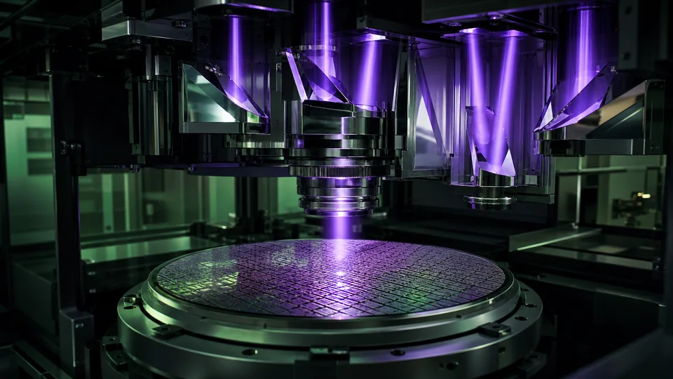
The pattern-transfer processes used to define nanoscale electronic structures repeatedly across semiconductor wafers.
SCIENDIA Knowledge Desk
Read article
A living academic reference written, refined and transparently versioned by the Sciendia community.
Collaborative knowledgeSearch
7 results
Wiki pages are public to read. Every signed-in member can create and improve them.
Clear searchThe pattern-transfer processes used to define nanoscale electronic structures repeatedly across semiconductor wafers.
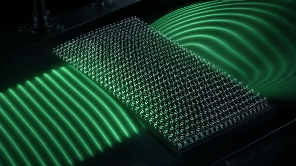
Engineered structures whose collective wave response is governed primarily by subwavelength geometry rather than bulk composition alone.
Chemical acceleration at an interface where reactants and catalyst occupy different physical phases.
A collective quantum state in which electrical resistance vanishes and magnetic response changes below critical conditions.
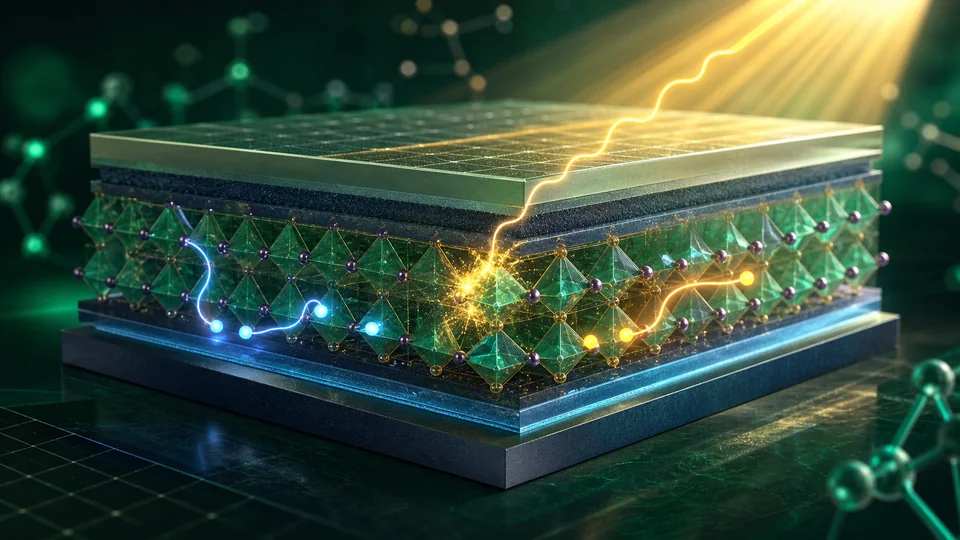
Thin-film photovoltaic devices built around halide-perovskite absorbers with tunable optoelectronic properties.
Quantum materials with an insulating bulk and robust conducting states at their surfaces or edges.
How electron transport and a proton gradient power ATP production across the inner mitochondrial membrane.